
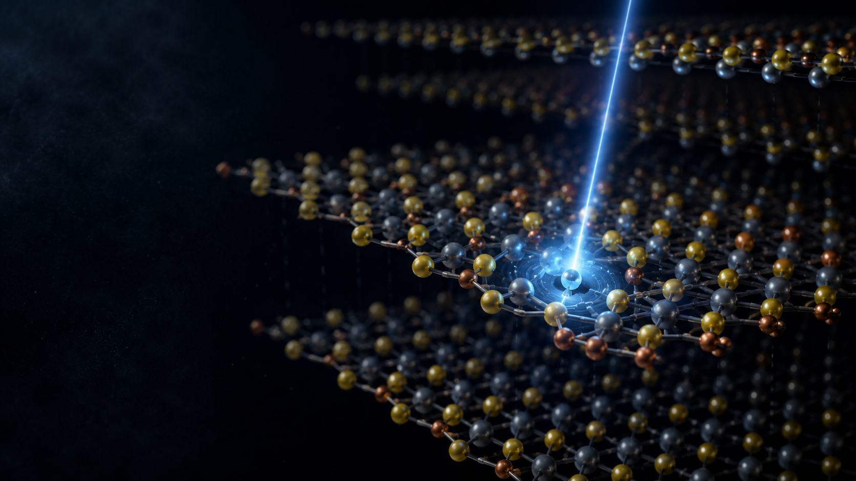
Defects have long shaped the behaviour of materials, often as random by-products of growth or processing. Julian Klein, Frances Ross, and collaborators have now used an electron beam to place defects in programmed arrays inside a crystal - turning imperfection itself into a scalable design tool for quantum, electronic, optical, and magnetic materials.
Electron microscopes are usually described as windows into the atomic world. They reveal the fascinating geometry of matter: rows of atoms, missing pieces, and tiny irregularities that can transform how a material behaves. But the electron beam that makes this hidden world visible also changes it.
For many researchers, that change is damage to be controlled. For Julian Klein, a physicist at the Massachusetts Institute of Technology, it became the beginning of an idea. Klein had spent years studying chromium sulfur bromide, or CrSBr, a layered magnetic semiconductor whose atoms seemed unusually willing to shift under the electron beam. Working with Frances Ross, MIT’s TDK Professor of Materials Science and Engineering and an expert in electron microscopy, he began to ask whether that movement could be turned from an unwanted side effect into a method for engineering matter.
Klein had been recording images of CrSBr when he and his collaborators noticed something striking. Under broad electron-beam exposure, chromium atoms in the crystal began to move. At first, the motion looked like a familiar problem in electron microscopy: the beam was altering the sample it was meant to observe. Yet that movement also suggested a possibility. If the atoms were already shifting, could they be moved deliberately?
The answer is now a demonstration of mesoscale atomic engineering: using an electron beam to steer chosen chromium atoms in CrSBr into selected sites inside the crystal without disrupting the structural integrity of the crystal. In doing so, the team created more than 40,000 user-defined defects in a small crystal volume.¹
Let's be clear: Defects have always been written into materials by growth conditions, processing, irradiation, impurities, or strain. Instead, what is different is control: the defects are placed in programmed arrays, rather than appearing randomly, and are created by manipulating atoms inside the body of a crystal, rather than rearranging those on the surface.
For Klein, the motivation began with the promise of a single imperfection. “If you have a single imperfection in a crystal, then you can have interesting properties,” he says. A defect can behave as a highly localized object, with electronic or optical behaviour of its own that is distinct from that of the rest of the crystal. In some materials, defects can emit single photons, making them attractive for quantum technologies. However, creating such objects with precision, and creating them inside a crystal, where they are less exposed to disturbances from the outside world, has remained difficult.
CrSBr offered the opportunity because its chromium atoms responded to the electron beam in an unusually helpful way. The material is described as a van der Waals magnetic semiconductor and its optical and magnetic properties have made it useful for studying low-dimensional physics.² But for this project, its crucial feature was rearrangement. Klein says the defining moment for studying this material was observing chromium atoms shift under electron exposure. Once that motion was visible, the next question followed naturally: could researchers target one atomic column and make only selected atoms move?
Answering that question required unusual precision. Electron microscopes have existed for decades, but placing a focused beam on a selected atomic site remains difficult. The team, in which Klein worked with Dr Kevin Roccapriore on state of the art electron microscopes at Oak Ridge National Laboratory (a US Department of Energy user facility), first had to develop a method for targeting atomic columns with sub-20-pm precision - 20 picometers being only a fraction of the distance between neighbouring atomic columns in a crystal.³
For Klein, that capability was “a very big step forward.” Still, positioning the beam was only part of the solution. The team also found that combining precise placement with a small directional scan could move atoms in chosen directions. “You could actually see how you could move the intensity from one atom column into a new atom column in a repeated manner,” he says. That was when the experiment revealed what he calls “this crazy control” over atomic displacement.
The breakthrough did not arrive in one triumphant day. Rather, Klein says, it came through “many, many tiny steps” pursued over several years to deliver electrons to exactly the right place.
Ross sees the result as part of a longer story in microscopy. “Right from the earliest days of electron microscopy, microscopists realized that the electron beam changes the sample,” she says. As microscopes improved, with finer beams and more accurate steering, researchers began asking whether those changes could be made deliberate.
There is historical precedent for moving atoms. In a famous 1990 experiment, IBM researchers used a scanning tunnelling microscope to position xenon atoms on a nickel surface. ⁴ But surface atoms are exposed and delicate, often requiring low temperatures and high vacuum to stay in place. By contrast, the CrSBr defects form within the crystal. “Unlike surface atoms that are sensitive to the environment and must be preserved in vacuum and at low temperatures, these engineered defect arrays are robust and stable in air,” Ross says. Because the defects are embedded in the crystal, the sample can be removed from the microscope and studied with other techniques. In that sense, the work moves atom manipulation closer to practical materials science, rather than keeping it as a delicate surface demonstration.
The larger significance, Ross says, is scale. A single defect may be useful, but arrays of defects can interact. In CrSBr, she says, each engineered defect acts “in some way like an artificial atom,” with energy levels and transitions that can be observed. Therefore, placing many such atom-like localized defects close together gives researchers a way to study how they influence one another.
One possible direction is quantum simulation. Unlike a general-purpose quantum computer, a quantum simulator is designed to emulate aspects of a specific quantum system that is difficult to calculate classically. Ross imagines writing a defect pattern whose interactions resemble those of a complicated molecule, then measuring how the material responds.
“It’s not really quantum computing,” Ross says. “Don’t give people the idea that we can solve every quantum computing problem.” Instead, the goal would be to write an array of defects that shares the interaction physics of a chosen problem and then study what that engineered material does.
The method could also allow physicists to explore patterns that nature would not ordinarily provide. Klein says researchers need not write only neat grids. They could deliberately introduce disorder or irregularity - structures “the human mind would not intuitively figure out” - to search for unusual magnetic, optical, or electronic effects. As a result, designed disorder could provide a route to probing elusive quantum phases or collective states of matter.
For now, the technique remains far from science-fiction materials that reshape themselves at human scales. Ross is cautious about comparisons to an Iron Man suit (Yes! I did ask that question. Don’t judge me, the child within was curious.) Strong, macroscopic structural materials are not the near-term goal. A more plausible path, she says, is toward new control systems and electronic materials: devices that use less power, perform new functions, or behave more like the human brain.
Even that path depends on whether the method can move beyond CrSBr. The microscope can, in principle, deliver electrons to selected places in many crystals. But the material must cooperate. Some crystals may rearrange usefully. Others may simply be damaged. CrSBr, Ross says, has been unusually “helpful and friendly.”
For Klein, the project began with an unexpected movement of atoms and became, through years of careful refinement, a way to arrange defects with intent. “It’s good to work on something for extended periods of time and dig really deep,” he says.For Klein, the project began with an unexpected movement of atoms and became, through years of careful refinement, a way to arrange defects with intent. “It’s good to work on something for extended periods of time and dig really deep,” he says.
Ross finds beauty in that slow unfolding. She says all crystals are beautiful, but what she likes most is watching them grow or transform: germanium on silicon, silicon nanowires from catalysts, a metal becoming an oxide or hydride. Such movies show atoms moving into their final positions.
In this work, the microscope has become part of the story itself: an instrument that sees the crystal, touches it, and, atom by atom, begins to write.
References
J. Klein, K. M. Roccapriore, M. Weile, S. Grytsiuk, A. R. Lupini, Z. Sofer, D. Pashov, M. van Schilfgaarde, S. Acharya, M. Rösner, and F. M. Ross, “Mesoscale atomic engineering in a crystal lattice,” Nature 653, 715–722 (2026). DOI: 10.1038/s41586-026-10431-9.
J. Klein et al., “The bulk van der Waals layered magnet CrSBr is a quasi-1D material,” ACS Nano 17, 5316–5328 (2023). DOI: 10.1021/acsnano.2c07316.
K. M. Roccapriore, F. M. Ross, and J. Klein, “Quantitative electron beam-single atom interactions enabled by sub-20-pm precision targeting,” Advanced Science 12, e02551 (2025). DOI: 10.1002/advs.202502551.
D. M. Eigler and E. K. Schweizer, “Positioning single atoms with a scanning tunnelling microscope,” Nature 344, 524–526 (1990). DOI: 10.1038/344524a0.